Odisha signs semiconductor MoU with Intel and 3DGS
Odisha signed a Memorandum of Understanding with Intel and 3D Glass Solutions on 28 and 29 May 2026 to bring substrate manufacturing technology to India. The agreement is linked to semiconductor packaging and advanced glass-based integration at Info Valley in Bhubaneswar, Khordha district.
Semiconductor packaging and glass substrates
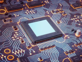
Semiconductor packaging is the process of enclosing and connecting integrated circuits for use in electronic systems. Glass substrates are used in advanced packaging because they support high-density interconnections in heterogeneous integration and 3D packaging.
India Semiconductor Mission and project structure
The project was approved under the India Semiconductor Mission in August 2025. It is being implemented by 3D Glass Solutions Inc., USA, through its wholly-owned Indian subsidiary, Heterogeneous Integration Packaging Solutions Private Limited.
Project cost, support and output
The total project cost is estimated at Rs 1,943.53 crore. Central government fiscal support is Rs 799 crore, and additional state support is about Rs 399.5 crore. The facility is expected to produce about 70,000 glass substrates annually, 50 million assembled units, and nearly 13,000 advanced 3D heterogeneous integration modules.
Applications and industrial context
The unit will focus on advanced 3D heterogeneous integration for artificial intelligence, high-performance computing, defence electronics, and next-generation telecom systems. Commercial production is expected to begin by August 2028.
Important Facts for Exams
- India’s first Advanced 3D Glass Semiconductor Packaging Unit is located at Info Valley in Bhubaneswar, Odisha.
- 3D Glass Solutions Inc. is a United States-based company with an Indian subsidiary named Heterogeneous Integration Packaging Solutions Private Limited.
- The India Semiconductor Mission is a central government programme for semiconductor and display manufacturing in India.
- Compound semiconductors use materials such as silicon carbide and gallium nitride in high-power and high-frequency applications.
Related semiconductor projects in Odisha
Odisha is also scheduled to host India’s first commercial compound semiconductor fabrication unit by SiCSem Private Limited with UK-based Clas-SiC Wafer Fab. The groundbreaking for that unit is scheduled for June 2026.
| Related | |
|---|---|