Types of Semiconductor Materials and Their Applications
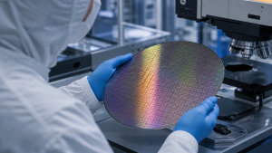
Semiconductor materials have electrical conductivity between that of conductors and insulators, and their conductivity can be controlled. Their properties make them essential to devices ranging from transistors and integrated circuits to LEDs, solar cells and high-frequency communication systems.
Semiconductor Fundamentals
A semiconductor is a crystalline or amorphous solid whose electrical conductivity can be altered. Its electronic band structure includes a band gap: an energy range in which electron states are absent. Conductors have overlapping valence and conduction bands, while insulators have large band gaps. Semiconductor band gaps are moderate, typically about 0.5–3.5 electron volts (eV).
- Temperature response: Conductivity generally increases with temperature, unlike in metals, as thermal energy enables more electrons to enter the conduction band.
- Charge carriers: Electrons in the conduction band and holes in the valence band carry electric current.
- Electronic uses: Controlling these carriers underpins transistors, diodes and integrated circuits.
- Material factors: Crystal structure and the number of valence electrons influence a semiconductor’s properties.
Intrinsic and Extrinsic Semiconductors
Semiconductors are classified as intrinsic or extrinsic according to their purity and whether impurities have been added. Doping is the deliberate introduction of impurities to change electrical properties and increase conductivity.
- Intrinsic semiconductors: These are pure materials, such as silicon and germanium. At absolute zero, they behave as insulators. At room temperature, thermal energy can excite some electrons into the conduction band, leaving holes behind. The numbers of free electrons and holes are equal.
- N-type semiconductors: Doping with a pentavalent Group 15 element, such as phosphorus, arsenic or antimony, supplies an additional electron. Electrons are the majority carriers and holes are the minority carriers.
- P-type semiconductors: Doping with a trivalent Group 13 element, such as boron, gallium or indium, creates holes in the bonding structure. Holes are the majority carriers and electrons are the minority carriers.
Elemental Semiconductors
Elemental semiconductors consist of a single element. Silicon and germanium are the most prominent examples, though their properties and uses differ.
- Silicon (Si): The most widely used semiconductor material, it accounts for over 90% of semiconductor devices. Abundant in nature, it occurs primarily as silica (silicon dioxide). Silicon has an indirect band gap, good thermal properties and a stable native oxide (SiO2), making it suitable for MOSFET fabrication. Uses include microprocessors, RAM and ROM, solar cells, power transistors and consumer-electronics integrated circuits.
- Germanium (Ge): An early semiconductor, it has a smaller band gap and higher electron mobility than silicon, but poorer thermal stability and no stable native oxide. It is used in infrared optics, high-frequency applications and specialised transistors. Silicon-germanium (SiGe) alloys can improve performance in high-speed circuits.
Compound Semiconductors
Compound semiconductors combine two or more elements, often from different periodic-table groups, such as Group III–V or Group II–VI elements. Many have direct band gaps that support efficient light emission. Wide-bandgap materials are suited to high-power or high-temperature applications.
- Gallium arsenide (GaAs): A III–V compound with a direct band gap, high electron mobility and strong high-frequency performance. Its applications include LEDs, laser diodes, microwave integrated circuits for radar and satellite communication, and high-efficiency solar cells, particularly for space applications.
- Gallium nitride (GaN): A wide-bandgap III–V material with high breakdown voltage, high power-handling capability and operation at high temperatures. It is used in blue and white LEDs, high-power radio-frequency devices for 5G networks, electric-vehicle power electronics and fast chargers.
- Silicon carbide (SiC): A wide-bandgap IV–IV compound with high thermal conductivity, high breakdown voltage, radiation hardness and mechanical robustness. Uses include high-power and high-frequency devices, electric-vehicle chargers, industrial motor drives, railway systems and high-temperature electronics.
- Indium phosphide (InP): A III–V semiconductor with a direct band gap and high electron velocity. It is used in high-speed fibre-optic communication, laser diodes, photodetectors and other optoelectronic devices.
Organic Semiconductors and Chip Manufacturing
Organic semiconductors are carbon-based compounds with semiconductor properties. Their flexibility, light weight, tunable electronic properties and potential for low-cost, solution-based processing make them useful for emerging applications. Improving efficiency and stability remains an area of research.
- Applications: Organic light-emitting diodes (OLEDs) are used in displays and lighting; organic photovoltaic cells (OPVs), flexible electronics, sensors and wearable devices are other applications.
- Fabrication stages: Semiconductor manufacturing involves deposition, removal, patterning and modification of electrical properties.
- Cleanrooms: Dust, vibration, temperature and humidity are controlled. Vibration damping helps photolithography machines achieve nanometre-scale alignment.
- Packaging and testing: Packaging encases the integrated-circuit die, protects it from physical damage and corrosion, and provides contacts to a circuit board. Testing follows packaging.
- Broader concerns: Semiconductor development involves critical-materials security, research and innovation, and resource sustainability.
Key Prelims Takeaways
- Semiconductor conductivity lies between that of conductors and insulators and generally rises with temperature.
- Intrinsic materials are pure; extrinsic materials are doped to alter conductivity.
- Pentavalent dopants produce N-type material with electrons as majority carriers; trivalent dopants produce P-type material with holes as majority carriers.
- Silicon is widely used because of its abundance, thermal properties and stable native oxide.
- Germanium has higher electron mobility than silicon but poorer thermal stability.
- GaAs is used in light-emitting and high-frequency devices; GaN and SiC support high-power applications.
- Organic semiconductors are used in OLEDs and flexible electronics; chip fabrication includes deposition, removal, patterning and electrical modification.
Recent Context
On November 6, 2026, web applications opened under Semicon India 2.0 for semiconductor machinery and materials, new fabrication plants, and ATMP/OSAT projects. Approved on July 15, 2026, with an outlay of ₹1,27,500 crore, the programme aims to attract at least 200 chip-design startups and companies.
| Related | |
|---|---|