Important Semiconductor and Chip Design Terms
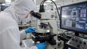
Semiconductors are the foundation of modern electronics, from microchips and memory to power systems and advanced communication hardware. Their materials, fabrication methods, chip designs, and packaging techniques determine performance, efficiency, and manufacturing scale.
Semiconductor Materials Overview
Semiconductor materials have electrical conductivity between that of conductors and insulators. They are selected on the basis of bandgap energy, temperature tolerance, and electron mobility.
Elemental Semiconductors
- Silicon (Si): The main material used in modern integrated circuits. It is abundant, structurally stable, and cost-effective to process.
- Germanium (Ge): A semiconductor with higher electron mobility than silicon. It was used in early transistors and is still common in infrared optics and high-speed photodetectors.
Compound and Wide-Bandgap Semiconductors
- Gallium Arsenide (GaAs): A compound semiconductor with very high electron mobility. It is suited for ultra-high-frequency applications such as satellite communications.
- Silicon Carbide (SiC): A wide-bandgap semiconductor that handles high voltage, elevated temperatures, and high power levels. It is used in industrial power electronics and electric vehicle drive systems.
- Gallium Nitride (GaN): A wide-bandgap material with high electron velocity and thermal conductivity. It is used in radiofrequency hardware, high-power military radars, and compact fast-charging adapters.
| Material | Bandgap Energy (eV) | Electron Mobility (cm²/V·s) | Key Applications |
| Silicon (Si) | 1.12 | 1,400 | General-purpose microprocessors, memory chips, analog circuits |
| Germanium (Ge) | 0.66 | 3,900 | High-speed photodetectors, fiber optic systems, solar panels |
| Gallium Arsenide (GaAs) | 1.42 | 8,500 | Radiofrequency components, optoelectronics, space-grade solar cells |
| Silicon Carbide (SiC) | 3.26 | 900 | High-voltage electric vehicle power systems, power grids, rail traction |
| Gallium Nitride (GaN) | 3.40 | 2,000 | Consumer electronics chargers, high-frequency radar, LEDs |
Core Fabrication and Manufacturing Processes
Microchip fabrication involves precise physical and chemical processing on thin wafers of high-purity silicon.
Substrates and Patterning
- Silicon Ingot: A single, large cylindrical crystal of ultra-pure silicon grown from molten silicon using methods such as the Czochralski process.
- Silicon Wafer: A thin, circular disc sliced from a silicon ingot. It serves as the base layer on which circuit patterns are printed.
- Photolithography: A printing method that projects light through a photomask to transfer microscopic patterns onto a wafer coated with photoresist.
- DUV (Deep Ultraviolet) Lithography: An optical projection system using light wavelengths of 193 nm or 248 nm. It is used for mature process nodes and mid-range microchips.
- EUV (Extreme Ultraviolet) Lithography: An advanced patterning system using a short wavelength of 13.5 nm. It is critical for features below 7 nm on silicon.
Physical and Chemical Processing
- Doping: The controlled injection of trace impurities, such as boron (p-type) or phosphorus (n-type), into silicon to modify its electrical behavior.
- Etching: The selective removal of material from the wafer surface to form trenches and lines. It is done through wet etching or dry etching.
- Chemical Vapor Deposition (CVD): A chemical process used to deposit thin films of crystalline or amorphous materials onto a wafer substrate.
- Cleanroom: A dust-free manufacturing environment classified by airborne particle concentration. Advanced microchip manufacturing requires ISO Class 1 conditions.
Semiconductor Design and Logic Structures
Chip design defines the physical layout, logical connections, and instruction capabilities of an integrated circuit.
Chip Architecture Types
- Integrated Circuit (IC): An assembly of interconnected active and passive electronic components fabricated onto a single monolithic piece of silicon.
- System on Chip (SoC): A single integrated circuit containing the main components of an electronic system, including a CPU, GPU, memory controller, and wireless radios.
- Application-Specific Integrated Circuit (ASIC): A microchip customized for a dedicated purpose, such as specific artificial intelligence algorithms, rather than general processing.
- Field Programmable Gate Array (FPGA): An integrated circuit designed to be configured and programmed by the purchaser after manufacturing is complete.
Design and Logic Instruction
- Electronic Design Automation (EDA): Software used to model, simulate, lay out, and verify the electrical performance of complex microchip designs.
- Instruction Set Architecture (ISA): The interface between software and hardware defining the basic operations, registers, and data types a chip can process. Common architectures include x86, ARM, and RISC-V.
Evolution of Transistor Geometries
Transistors act as electrical switches within microchips. Their architecture has evolved to reduce leakage currents as physical features shrink.
- Planar MOSFET: A traditional flat transistor layout where current flows horizontally across the silicon surface under a single flat gate.
- FinFET (Fin Field-Effect Transistor): A three-dimensional design where the silicon channel is raised as a vertical fin. The gate wraps around three sides of the fin, reducing unwanted current leakage.
- GAAFET (Gate-All-Around FET): An advanced design where the channel is built from horizontal nanosheets completely surrounded by the gate material on all four sides.
| Transistor Type | Structure | Gate Control Mechanism | Ideal Process Nodes |
| Planar MOSFET | Two-dimensional horizontal channel | Gate sits on top of the horizontal channel | 28 nm and above |
| FinFET | Three-dimensional vertical channel (fin-like) | Gate wraps around three sides of the vertical channel | 22 nm down to 3 nm |
| GAAFET | Stacked horizontal nanosheets/nanowires | Gate surrounds the channel on all four sides | 3 nm and below |
Advanced Packaging and Assembly Methods
Advanced packaging joins multiple functional dies in one physical assembly to increase circuit density without changing the underlying silicon lithography.
- Die: A single, unpackaged rectangular block of functional circuitry diced from a completed silicon wafer.
- Chiplet: A small, modular integrated circuit die designed to perform specific sub-functions. Multiple chiplets are linked together to work as a unified processor.
- Through-Silicon Via (TSV): A microscopic vertical electrical conduit passing through a silicon die, enabling fast signals between stacked chips.
- 2.5D Packaging: An assembly method where multiple dies or chiplets are placed side by side on a thin silicon interposer layer that routes signals between them.
- 3D Packaging: An assembly process where multiple silicon dies are stacked directly on top of each other using TSVs, minimizing physical footprint.
Global Semiconductor Industry Models
The semiconductor supply chain is divided into specialized corporate roles based on design, fabrication, or assembly functions.
- Integrated Device Manufacturer (IDM): A semiconductor company that performs designing, fabricating, testing, and packaging in-house.
- Fabless Company: A firm that develops, designs, and markets chips but outsources manufacturing to specialized production facilities.
- Pure-play Foundry: A manufacturing facility that produces chips exclusively for external clients, without designing or marketing its own products.
- OSAT (Outsourced Semiconductor Assembly and Test): Third-party service providers that package, assemble, and test raw silicon dies before shipment.
Operational Principles and Performance Indicators
Semiconductor manufacturers track several technical metrics to evaluate efficiency, speed, and commercial viability.
- Process Node: A reference term for specific manufacturing generations. Earlier it denoted actual transistor gate length, but now it is largely a comparative technology label.
- Yield: The percentage of functional, error-free chips produced on a wafer compared to the total theoretical capacity of that wafer.
- PPA (Power, Performance, Area): The three design parameters representing energy use, operating speed, and physical silicon footprint.
- Moore’s Law: An empirical observation that the number of transistors on a microchip doubles roughly every two years.
Recent Context
NIELIT will set up India’s first dedicated Quantum and AI University campus in Amaravati, with MeitY funding and a focus on semiconductor fabrication, chip design, VLSI, and related advanced technologies. The project reflects India’s push for manufacturing capability and supply chain resilience.
Rare Facts for Prelims
- Silicon’s advantage: It naturally forms a stable oxide layer, silicon dioxide, which is crucial for transistor manufacturing.
- Germanium comeback: Germanium is being explored again in advanced chip research because it can support faster carrier movement than silicon.
- GaN on the rise: Gallium nitride is especially useful for compact power chargers because it can switch rapidly with lower energy loss.
- TSV importance: Through-silicon vias are one of the main enablers of modern chip stacking and memory integration.
- FinFET shift: FinFETs were adopted to control leakage at very small process nodes where planar transistors became less efficient.
- Cleanroom sensitivity: Even tiny airborne particles can damage nanoscale chip features, making contamination control critical in fabs.
| Related | |
|---|---|