Types of AI Chips and Computing Accelerators
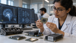
AI chips are processors designed to accelerate the computations used in artificial intelligence and machine learning. Their architectures support parallel processing and can improve performance or energy efficiency compared with general-purpose processors. Different accelerators suit different stages and workloads, from model training to inference.
Understanding AI Chips and Accelerators
AI chips are integrated circuits or specialised processors optimised for computations common in AI algorithms, including matrix multiplication, convolutions and neural-network operations. Unlike a CPU, which handles a broad range of tasks, an accelerator is designed to perform particular operations efficiently, often in parallel. The choice of hardware depends on the workload, including its scale, precision requirements, power limits and need for flexible programming. Accelerators support the computation demands of applications such as computer vision and natural language processing.
- Training: Uses data to develop a model and can involve large volumes of repeated calculations.
- Inference: Applies a trained model to new data, often with requirements for efficiency or low latency.
Graphics Processing Units (GPUs)
GPUs were originally designed to render computer graphics and video games. Their architecture, with many processing cores working in parallel, also makes them useful for the large-scale calculations involved in AI.
- Parallel processing: Thousands of cores can perform many calculations simultaneously, making GPUs effective for deep-learning training and matrix operations.
- Programming: NVIDIA’s CUDA platform is a widely used programming model for GPU-based AI applications.
- GPGPU: General-Purpose computing on Graphics Processing Units uses GPUs for calculations beyond graphics rendering.
Application-Specific Integrated Circuits and TPUs
An application-specific integrated circuit (ASIC) is custom-built for a particular application or task. Its specialised design can deliver high performance and power efficiency for its intended function. This focus comes with a trade-off: ASICs are generally less flexible than general-purpose processors, and their design and manufacture can be expensive. They are particularly efficient for inference, where a trained model is applied to new data. Google’s Tensor Processing Unit (TPU) is an ASIC and a neural-processing unit (NPU), developed for neural-network machine-learning workloads. Compared with GPUs, TPUs favour high-volume, low-precision computation and offer more input/output operations per joule. They do not include graphics-rendering hardware.
- Systolic array: Google selected this design after three separate groups developed AI accelerators. Thousands of multiply-accumulators connect directly to one another, moving data in a rhythmic flow and reducing memory access during matrix multiplication.
- Precision: The second-generation TPU added floating-point computation to integer processing and introduced bfloat16. This lightweight floating-point format retains the range of FP32 with fewer mantissa bits, enabling both training and inference.
- TPU 8tx: This system shares silicon with TPU 8t and is paired with fifth-generation AMD EPYC CPU hosts. It is designed for secure, confidential inference and small-scale training, using hardware-level security to protect data and AI models during processing.
- TPU 8i Max: Designed for memory-intensive workloads, including large context windows and AI agents processing extensive codebases or lengthy videos, it provides twice the computing capacity and memory bandwidth of TPU 8i.
- Software access: Google open-sourced TorchTPU in October 2026, enabling PyTorch code and Hugging Face models to run natively on its chips. An open-source TPU agent suite is in preview; it supports Claude Code, Cursor and Google Antigravity, and automates onboarding and custom-kernel optimisation.
- Deployment: Customers can access TPUs through Google Cloud or deploy them in their own data centres. The TPU business serves nearly 100 customers, including AI laboratories, trading firms, retailers and universities.
Field-Programmable Gate Arrays
Field-programmable gate arrays (FPGAs) are reconfigurable integrated circuits that can be programmed or reprogrammed after manufacture. They offer a balance between GPU flexibility and ASIC efficiency, allowing their configuration to suit specific functions.
- Prototyping: FPGAs can be used to develop and test AI accelerators before a fixed design is adopted.
- Edge computing: They suit some applications requiring low latency and custom data pipelines.
- Adaptability: Their reconfigurability, versatility and power efficiency can support specialised deep-learning use cases.
Emerging Architectures and Broader Relevance
Other approaches seek to reduce energy use or data movement, or to change how computations are performed. They represent distinct architectural ideas rather than interchangeable chip types.
- Neuromorphic chips: Inspired by the human brain, they aim for energy-efficient, event-driven processing and integrate memory with computation to reduce data movement.
- Analog AI chips: These use analog rather than digital signals and may improve speed and power efficiency by reducing data conversion and movement. IBM’s analog AI chips use phase-change memory (PCM).
- In-memory computing: Processing takes place directly in memory units, reducing movement between processor and memory to improve speed and efficiency for AI workloads.
The range of accelerators also highlights broader technology considerations: building indigenous technology capacity, strengthening digital infrastructure and supporting research and development. These areas matter when assessing the development and deployment of specialised computing hardware.
Key Prelims Takeaways
- AI chips: Specialised hardware accelerates AI and machine-learning computations.
- GPUs: Their parallel architecture supports deep-learning training and large-scale matrix operations.
- ASICs: Custom designs offer efficiency for targeted tasks but generally have less flexibility and higher design costs.
- TPUs: Google’s ASICs and NPUs are designed for neural-network machine learning and use a systolic-array architecture.
- FPGAs: Reconfigurable chips are useful for prototyping and specialised low-latency applications.
- Emerging approaches: Neuromorphic, analog and in-memory computing seek to reduce energy use or data movement through different architectures.
Recent Context
On November 9, 2026, Google launched TPU 8tx and TPU 8i Max, expanding its eighth-generation portfolio alongside TPU 8t for large-scale training and TPU 8i for inference and real-time reasoning. It was the first year Google introduced four TPU systems.
| Related | |
|---|---|