Tamil Nadu Launches Semiconductor Ecosystem Policy
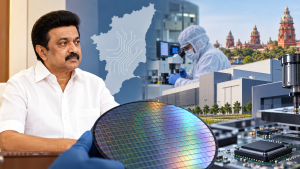
Tamil Nadu Chief Minister C. Joseph Vijay launched the Tamil Nadu Semiconductor Ecosystem Policy at the Secretariat in Chennai on October 15, 2026. The policy aims to position the state as a leading hub for semiconductor and advanced electronics manufacturing in India.
Incentives across semiconductor segments
The policy proposes additional state incentives for investment projects approved under the Union government’s Semicon India Programme 2.0, as well as tailored support for eligible projects important to Tamil Nadu’s semiconductor ecosystem that may fall outside the Union scheme. State subsidies of up to 25% are available for eligible capital expenditure. The policy provides 25% state support for 300-mm silicon semiconductor wafer fabrication projects, alongside the Centre’s 40% financial assistance. Advanced packaging projects can receive 25%, legacy packaging projects 20%, and projects involving semiconductor materials, testing, equipment research and development 15%. Minimum investment thresholds vary by segment, from ₹50 crore to ₹500 crore.
Important Facts for Exams
- Cleanroom controls: Wafer-fabrication fabs require tightly controlled cleanrooms: dust can ruin nanoscale circuits, while vibration, temperature and humidity control support precise photolithographic alignment.
- Packaging role: Integrated-circuit packaging encloses a die against physical damage and corrosion, provides contacts to connect it to a circuit board, and precedes device testing.
- Area-array design: Area-array packages distribute interconnection terminals across the package surface, enabling more connections than designs that use only the outer perimeter.
| Related | |
|---|---|