SEMICON India 2026 Unveils Semicon 2.0 Roadmap
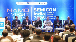
SEMICON India 2026 is being held from 17 to 19 September 2026 at Yashobhoomi, also called the India International Convention and Expo Centre, in Dwarka, New Delhi. The fifth edition of SEMICON India was inaugurated on 17 September 2026 by Prime Minister Narendra Modi, and the event covered India’s semiconductor policy, manufacturing, and design ecosystem.
Semicon 2.0 Framework
Semicon 2.0 is the next phase of India’s semiconductor programme and is structured around six pillars. These pillars are chip design, machines and materials, fabrication facilities, advanced packaging, applied research and development, and talent development.
The Union Cabinet approved Semicon 2.0 in July 2026 with an outlay of Rs 1.275 trillion, or US$13.23 billion. The programme expands government support across the semiconductor value chain, from design to manufacturing and packaging.
Investment and Industry Commitments
Investment commitments of about Rs 1 lakh crore, or US$11–12 billion, have been received under Semicon 2.0. These commitments are expected to materialise over the next two to three years.
Applied Materials announced a US$5 billion investment plan over the next decade under its India Vision 2035 programme. The plan covers research, supplier development, and talent development in India.
Employment and Start-up Support
Semicon 2.0 aims to create close to one lakh new jobs across the semiconductor ecosystem. The programme also targets 100,000 technicians for cleanroom and factory-floor roles.
The programme targets support for at least 200 chip-design start-ups and companies. In the first phase, 105 start-ups were supported, and 20 of them secured around Rs 800 crore in venture capital funding.
Important Facts for Exams
- Yashobhoomi is the India International Convention and Expo Centre in Dwarka, New Delhi.
- Semiconductors are used in chips for electronics, automobiles, telecom, defence systems, and industrial equipment.
- Advanced packaging is a post-fabrication process used to improve chip performance and integration.
- Applied Materials is a global company associated with semiconductor equipment and materials.
India’s Semiconductor Policy Context
India’s semiconductor programme includes support for design, fabrication, packaging, and research. The policy framework also includes skill development for technicians and engineers in the semiconductor supply chain.
Semicon India 2026 is the fifth edition of the annual event. The programme’s stated ecosystem focus includes start-ups, manufacturing units, and research-linked industry partnerships.
| Related | |
|---|---|