India’s Semiconductor Policy and Electronics Manufacturing Schemes
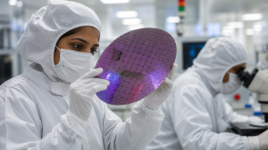
India’s semiconductor policy framework is designed to build a domestic ecosystem for chip design, fabrication, packaging and display manufacturing. The aim is to reduce import dependence, strengthen supply chains and encourage investment across the electronics value chain.
India Semiconductor Mission
The India Semiconductor Mission is the nodal agency for driving the country’s long-term semiconductor and display strategy. It supports the creation of a sustainable ecosystem through financial incentives, institutional coordination and research support.
- Strategic role: Formulates and implements policies for semiconductor and display manufacturing.
- Capital support: Provides fiscal assistance of up to 50% of project capital expenditure on a pari-passu basis for eligible projects.
- Coverage: Supports silicon CMOS fabrication, display fabs, compound semiconductors, silicon photonics, sensors, discrete semiconductor fabs and packaging units.
- Research focus: Encourages domestic R&D and technology development in advanced electronics.
- Skill development: Promotes specialised curricula in academic institutions to build a skilled workforce.
Major Incentive Schemes
India has created separate schemes for different segments of the semiconductor and electronics manufacturing ecosystem. These incentives are intended to attract private investment and reduce the cost burden of setting up high-capital projects.
| Scheme | Target area | Incentive structure |
| Modified Scheme for Semiconductor Fabs | Silicon CMOS-based fabrication plants | Up to 50% of project cost on a pari-passu basis |
| Modified Scheme for Display Fabs | Display fabrication facilities | Up to 50% of project cost on a pari-passu basis |
| Compound Semiconductor and ATMP Scheme | Packaging, testing, sensors and compound chips | Up to 50% of capital expenditure |
| Design Linked Incentive Scheme | Chip design startups and microprocessors | Product design incentives up to 50% of eligible expenditure |
Design, Packaging and Ancillary Ecosystem
The policy framework does not focus only on fabs. It also supports design-led growth, packaging, testing and domestic supply chain creation, which are essential for a complete electronics ecosystem.
- Design Linked Incentive Scheme: Supports fabless design startups through product design incentives and deployment-linked incentives based on net sales turnover.
- Chip design support: Encourages microprocessor and chip design activity within India.
- ATMP and packaging: Promotes assembly, testing, marking and packaging facilities.
- Ancillary industry: Targets electronic components, sub-assemblies and specialised chemicals to develop a domestic supply chain.
- Raw material base: Aims to reduce reliance on imported inputs for semiconductor manufacturing.
Implementation and Ground-Level Progress
The policy has already led to major investment commitments and project execution in several states. The effort is spread across fabrication, assembly and advanced manufacturing partnerships.
- States involved: Gujarat, Odisha, Uttar Pradesh and Rajasthan have emerged as important locations for semiconductor and related projects.
- Public-private model: Joint ventures and partnerships between domestic conglomerates and international technology firms support advanced node manufacturing.
- Manufacturing focus: The ecosystem includes fabrication units as well as assembly and testing facilities.
- Export potential: The broader strategy aims to place India on the global electronics manufacturing map.
Key Institutions and Support Systems
Several official institutions and support mechanisms have been created to help the ecosystem move from design to fabrication and prototyping.
- Semiconductor Laboratory, Mohali: Serves as a foundational research and fabrication facility for domestic prototype testing.
- Chips to Start up initiative: Provides academic institutions and startups access to electronic design automation tools.
- Academic linkages: Helps build a skilled talent pipeline for semiconductor design and manufacturing.
- R&D support: Strengthens indigenous capability in advanced electronics and chip development.
Key Prelims Takeaways
- India Semiconductor Mission: The nodal agency for semiconductor and display ecosystem development.
- Capital support: Eligible projects can receive up to 50% of project capital expenditure on a pari-passu basis.
- Major schemes: Semiconductor fabs, display fabs, Compound Semiconductor and ATMP, and Design Linked Incentive are the core schemes.
- Design support: The Design Linked Incentive Scheme supports chip design startups and microprocessor-related work.
- Outlay: The flagship national program was initially launched with an outlay of ₹76,000 crore.
- Research facility: The Semiconductor Laboratory in Mohali is important for prototype testing and fabrication support.
- Objective: The policy seeks technological sovereignty and reduced dependence on overseas semiconductor imports.
| Related | |
|---|---|