Fujifilm to Invest ₹800 Crore in Semiconductor Materials Facility
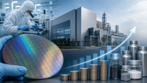
Fujifilm has announced a greenfield semiconductor materials manufacturing facility in India with a total investment of about ₹800 crore, or around USD 83 million. The project will be implemented in two phases, with Phase 1 scheduled to begin in October 2026 and commercial production expected in fiscal year 2028.
Semiconductor Materials
Semiconductor materials are specialised chemicals and inputs used in chip fabrication, packaging, and surface treatment. Front-end process chemicals are used in wafer-level manufacturing, while high-purity chemicals are required in processes that demand very low contamination levels.
Project Phases and Product Scope
Phase 1 of the facility will focus on front-end process chemicals for semiconductor production. Phase 2 will expand the plant into semiconductor surface conditioning materials and high-purity chemicals, with capacity planned to scale with market growth.
India Semiconductor Mission 2.0
The project aligns with India Semiconductor Mission 2.0, which was approved by the Government of India in July 2026. The mission is part of India’s policy framework for semiconductor manufacturing, design, and ecosystem development.
Important Facts for Exams
- Fujifilm is a Japanese multinational company known for imaging, materials, and advanced industrial solutions.
- A greenfield project is a new facility built on undeveloped land rather than an existing industrial site.
- Semiconductor fabrication uses ultra-clean chemicals, gases, and materials to maintain process precision.
- India Semiconductor Mission is a central policy initiative linked to semiconductor ecosystem development in India.
Supply Chain and Manufacturing Network
The facility is intended to strengthen local supply chain capabilities for advanced chip manufacturing in India. It will also integrate Fujifilm’s Indian operations into its global manufacturing network.
| Related | |
|---|---|