Tata Electronics Signs MoUs at Semicon India 2026
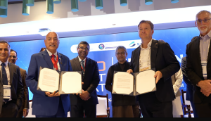
Tata Electronics announced multiple Memoranda of Understanding at Semicon India 2026 on 17–18 September 2026 for semiconductor manufacturing, materials supply, infrastructure support, packaging, and workforce development. The partnerships are linked to Tata Electronics’ facilities at Dholera in Gujarat and Jagiroad in Assam, which are part of India’s expanding semiconductor ecosystem.
Semiconductor Manufacturing Facilities
Tata Electronics is developing a fab at Dholera and an assembly and testing facility at Jagiroad. The Dholera unit is associated with front-end wafer fabrication, while the Jagiroad unit is associated with back-end assembly, testing, and advanced packaging. Nexperia, a Europe-based semiconductor company, was named in collaboration plans for front-end wafer fabrication of MOSFETs at Dholera and assembly and testing of discrete semiconductor products at Jagiroad. MOSFET stands for Metal-Oxide-Semiconductor Field-Effect Transistor and is a basic semiconductor device used in electronic circuits.
Strategic Partnerships for Materials and Infrastructure
Sumitomo Chemical, a Japan-based company, signed an MoU to support India’s semiconductor materials ecosystem through supply and possible local manufacturing of high-purity chemicals for the Dholera fab. High-purity chemicals are used in semiconductor processing, where contamination control is essential. Kelington, a Malaysia-based engineering company, partnered with Tata Electronics for critical infrastructure deployment, systems integration, engineering capabilities, and training of local talent. Such infrastructure support is required for cleanroom operations, utilities, and process readiness in semiconductor fabs.
Packaging, Design, and Skill Development
Enomoto Co. Ltd, a Japan-based company, entered into a partnership to strengthen advanced semiconductor packaging capabilities at the Jagiroad facility and to explore localisation of lead frame manufacturing. Lead frames are metal components used in semiconductor packaging to connect the chip to external circuits. Tata Electronics also identified collaborations with Semi-Conductor Laboratory and Gati Shakti Vishwavidyalaya for chip design services, technology node enablement, supply chain localisation, and workforce skilling. Semi-Conductor Laboratory is a Government of India semiconductor institution, and Gati Shakti Vishwavidyalaya is a central university focused on transport and logistics education.
Important Facts for Exams
- Semicon India is a national platform linked to India’s semiconductor manufacturing and ecosystem development.
- Dholera is in Gujarat, and Jagiroad is in Assam.
- MOSFET is one of the most widely used semiconductor devices in electronics.
- Lead frame manufacturing is part of semiconductor packaging technology.
Tata Electronics’ announced MoUs covered companies from Japan, Malaysia, Europe, and India. The partnerships included materials, infrastructure, packaging, design, and skilling components.
| Related | |
|---|---|