Samsung Affiliates Plan $9.15 Billion Semiconductor Investment
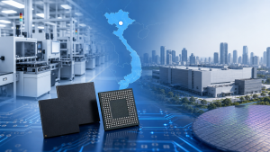
Samsung affiliates plan to invest a combined 12.26 trillion won (9.15 billion) in semiconductor operations in Vietnam and South Korea. About 8 trillion won (5.99 billion) is earmarked for Vietnam, while South Korea is to receive investment in high-end production capacity. The plans include memory-chip testing facilities and expanded flip-chip ball grid array substrate capacity.
Memory Chip Testing in Vietnam
Samsung Electronics plans to invest 105.79 trillion Vietnamese dong ($4.09 billion) in memory-chip testing facilities at Yen Binh Industrial Park in Thai Nguyen, northern Vietnam. The first production line is scheduled to start operations in the fourth quarter of 2027, with a second line planned for 2028.
The facilities will conduct final testing of DRAM and NAND flash chips packaged at Samsung’s Cheonan plant in South Korea. The investment expands overseas testing capacity; it does not include wafer manufacturing. Around 66.64 trillion dong ($2.58 billion), or 63 per cent of the Vietnamese facilities’ planned investment, is expected to come from reinvested profits generated by Samsung’s local operations.
DRAM is volatile memory that requires power to retain stored data, while NAND flash is non-volatile memory. High-bandwidth memory is a stacked memory technology used in applications including artificial intelligence computing.
FCBGA Substrate Capacity
Samsung Electro-Mechanics announced a 6.78 trillion won (5.08 billion) investment to expand production of flip-chip ball grid array (FCBGA) substrates. Of this amount, 4.27 trillion won (3.20 billion) is allocated to its Sejong facility in South Korea, and 2.51 trillion won ($1.88 billion) to Vietnam.
FCBGA substrates connect high-performance processors to circuit boards. They form part of semiconductor packaging, which protects and electrically connects a chip after wafer fabrication and testing. Samsung Electro-Mechanics plans to begin mass production at the expanded Sejong facility in September 2028; the Vietnamese expansion is targeted to operate by June 2030.
Semiconductor Operations and Production Locations
The Vietnamese testing facilities will handle final chip testing, while the chips will be packaged at Cheonan in South Korea. Samsung Electro-Mechanics plans to expand FCBGA substrate production at facilities in Sejong and Vietnam. The investment plans therefore cover separate parts of semiconductor production: memory-chip testing and substrate manufacturing.
Important Facts for Exams
- DRAM stands for dynamic random-access memory and is volatile memory.
- NAND flash is a non-volatile memory technology used in data storage.
- FCBGA stands for flip-chip ball grid array, a semiconductor package substrate format.
- Semiconductor production includes wafer fabrication, chip testing and packaging.
The first Vietnamese memory-chip testing line is scheduled to begin operations in the fourth quarter of 2027. Mass production at the expanded Sejong FCBGA facility is planned for September 2028.
| Related | |
|---|---|